Introduction
The Sipeed Tang Nano (sometimes also refered to as Lichee Tang Nano) is a cheap but powerful FPGA development0 board that features the GW1N-LV1QN48C6/I5 chip from Gowin. It costs as little as USD4.90 or CNY34.90. The Gowin GW1N chip has 1152 LUT4, 864 FF, 72Kbit B-SRAM, 96Kbit user flash and 1 PLL. The board also has an onboard 24MHz crystal. The board has 64Mbit QSPI PSRAM, 36 I/O Pins, 1 RGB LED, 2 push buttons and a 40-pin LCD interface with on-board backlight driver circuit. It has a built-in JTAG downloader so you can download to the chip by simply connecting the computer to it through a USB-Type-C cable.
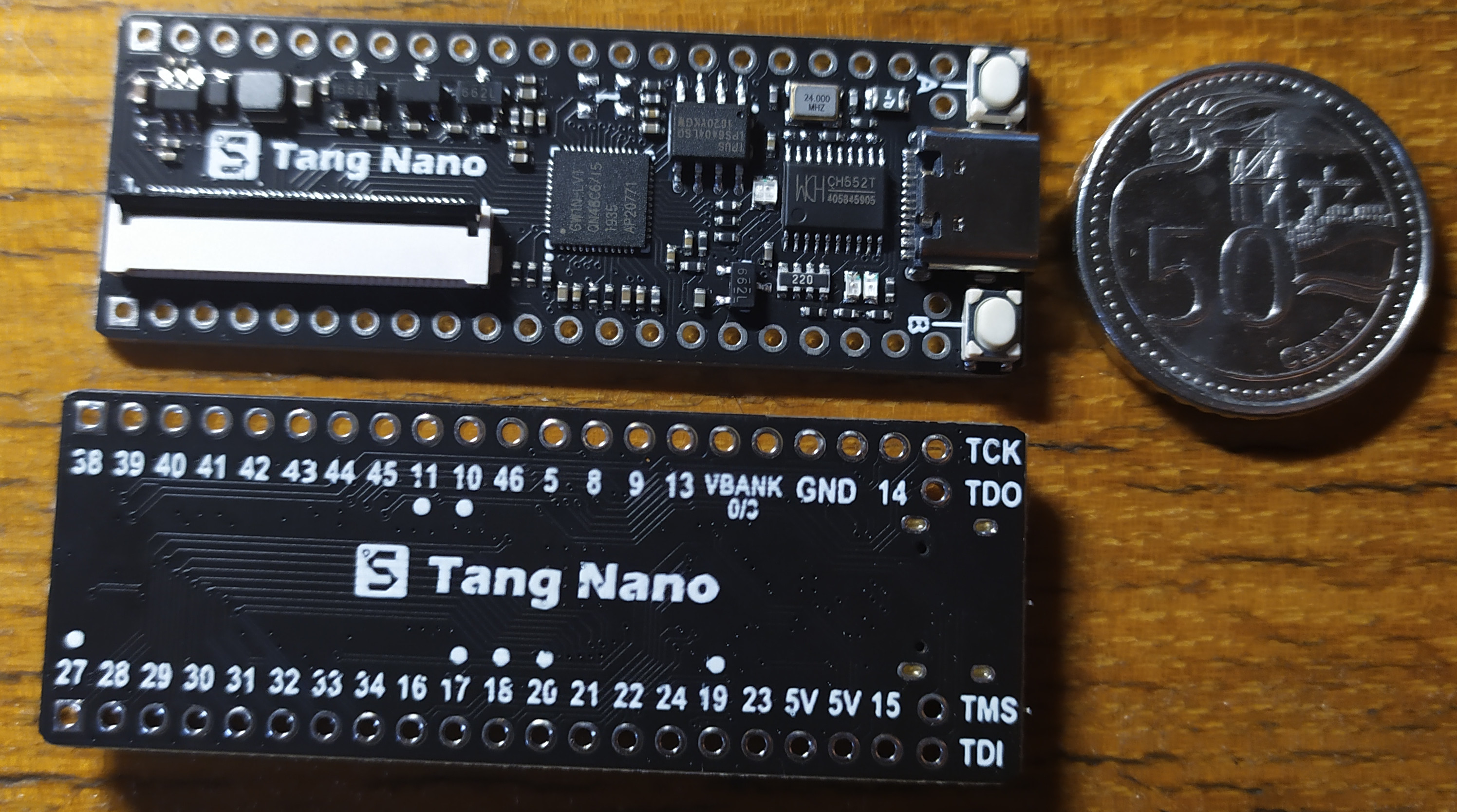
In this article, we will go through the basic steps of how to set up a development environment for the Tang Nano.
Download and Install the official Gowin IDE
For now, we need the official Gowin IDE to work with the Tang Nano board. Download the IDE from here. Find the links shown in the figure below and download the latest version for your operating system (Windows or Linux).

To install the IDE, Windows users need to unzip and run the installer and follow the step-by-step instructions. Install the driver if not already installed.
For Linux (I have only tested it on Ubuntu, but other common Linux distros should also work) users, just extract the files to any location.
Configure License
Open the IDE. Windows users can select it from the Start Menu and linux users can run the gw_ide executable file under the .../IDE/bin/ directory (make sure you have execute permission).
Upon starting, the software would prompt for license configuration. You can either use a local license or a license server. A local license allows you to use the software when you are offline. For now, just use Sipeed's license server to set it up. If you want to get a local license file, use the link at the bottom of the window or follow the instructions on this page. (Remember to check your SPAM folder!!!)
Fill in the following information:
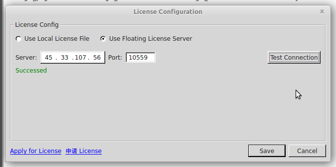
Press the Test Connection button and you should see a "Successed" (sic) message.
If you want to use the Synplify Pro synthesizer in the IDE, you also need to add an environment variable: [email protected].
On Windows, run the following command in cmd:
setx LM_LICENSE_FILE [email protected]
On Linux, append the following line to your ~/.bashrc or ~/.profile, etc.
export [email protected]
After entering the IDE, click on Synplify Pro under Tools. The synthesizer should be opened in a few seconds. If the license verification fails, try a re-login or reboot.
Try a Simple Design
Let's start with a basic design. Since the board has 2 push buttons and an LED, why not use the push buttons to light up the LED?
Let's take a look at the schematic of the board (link here).
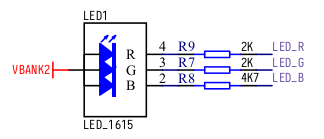
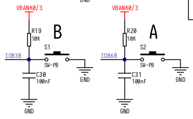
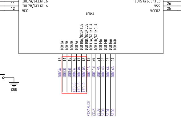
From the schematic, we can see that The cathode (negative side) of the R/G/B LED are connected to pins 18, 16 and 17 respectively. When you pull those pins low, the LED would light up. The two push buttons are connected to pins 14 and 15 which are normally pulled up. When a button is pressed, the corresponding pin would be pulled low. With these information, we can get started.
First, open the IDE.
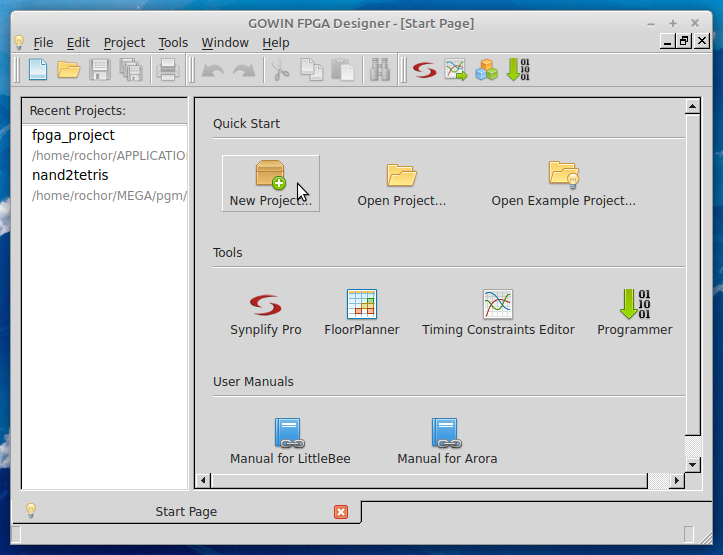
On the start page, create a new project by clicking on New Project... under Quick Start or File -> New.
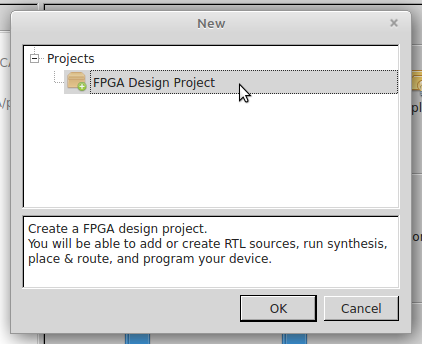
Choose FPGA Design Project.
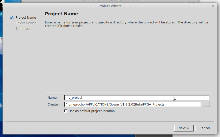
We'll name it 'my_project'. Choose a suitable directory to create your project in.
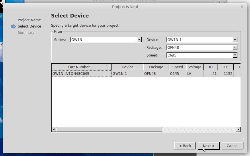
Select GW1N-LV1QN48C6/I5 from the list. It may be quicker to use the filters.
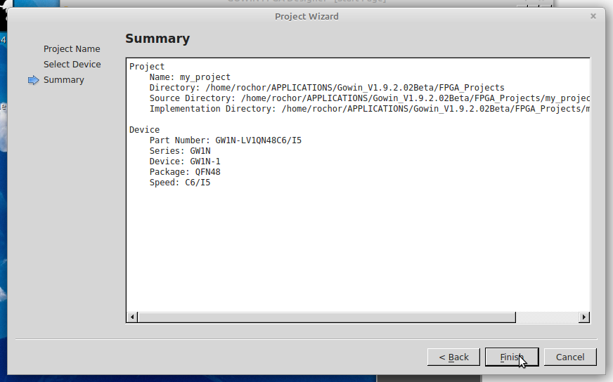
Finally, make sure all information on the summary page is correct and click on Finish. You will then be directed to a design summary page of your newly created project.
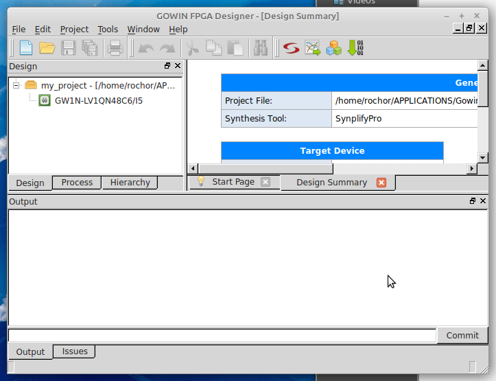
Within Design panel, right click and select New File...
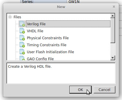
Choose Verilog File and click on OK.
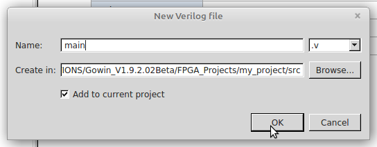
Give it a random name and click on OK again.
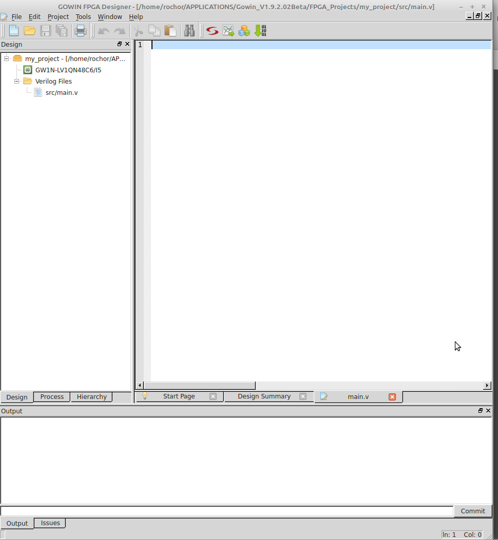
Now we are in the editor view.
Copy and paste the following code into the editor.
module main (
    input buttonA, buttonB,
    output led
);

nand (led, a, b);
not (a, buttonA);
not (b, buttonB);
endmodule;
The above code defines a module called main with 2 input ports and one output port. It can be illustrated in the figure below.
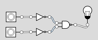
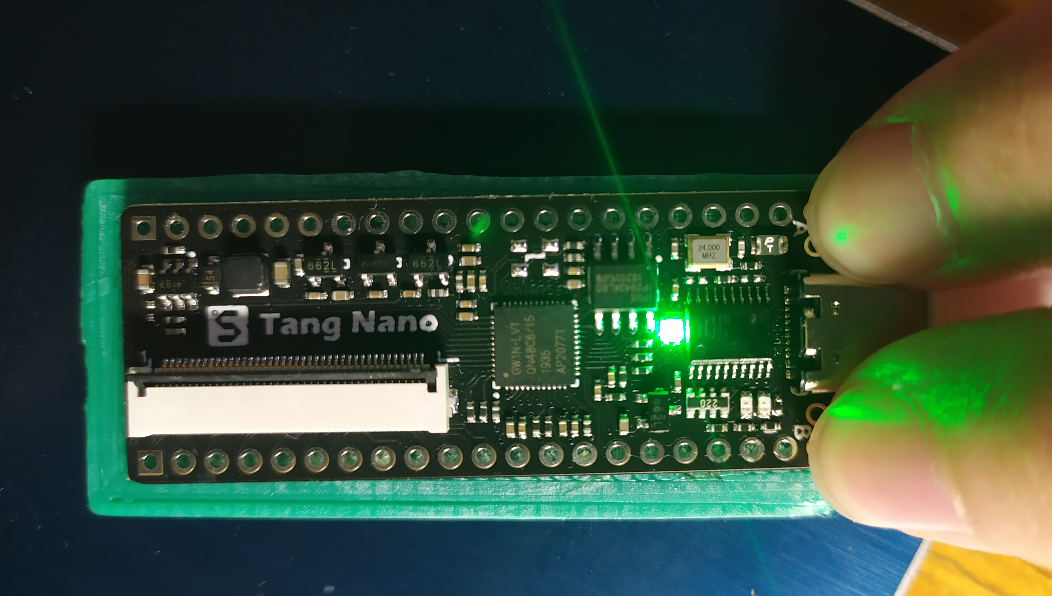
Note that only when both push buttons are pressed, their outputs will be pulled low and thus the inputs to the nand gate will be high after passing the inverters. The output of the nand gate (the cathode of the LED) will therefore be low, thus lighting up the LED.
Save the verilog file and go to Process panel.
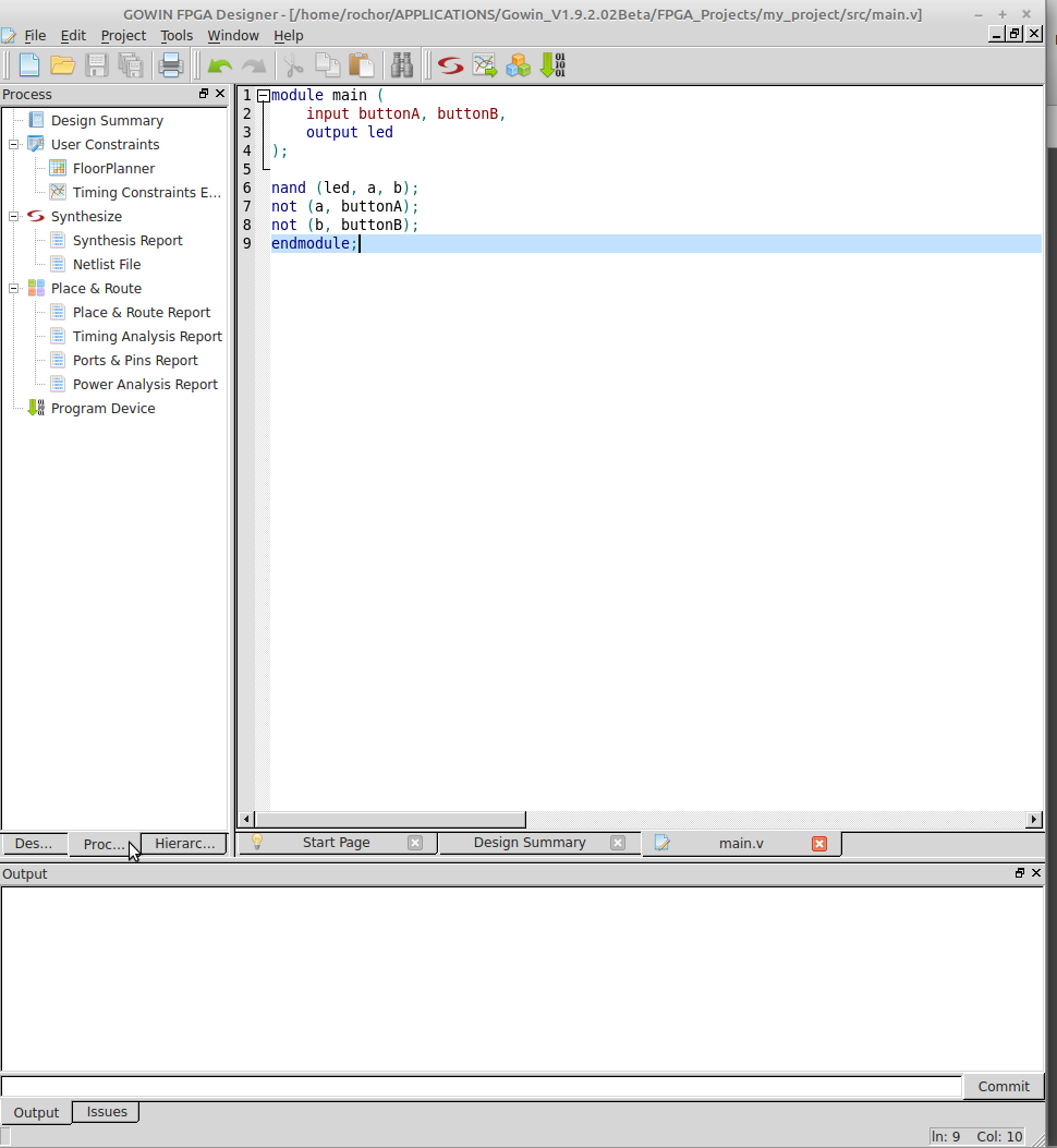
Right click on Synthesize -> Configuration.
You can use either the Synplify Pro or the GowinSynthesis as synthesizer. If you do not have a license for Synplify Pro, you should select GowinSynthesis. Leave everything else as default for now.
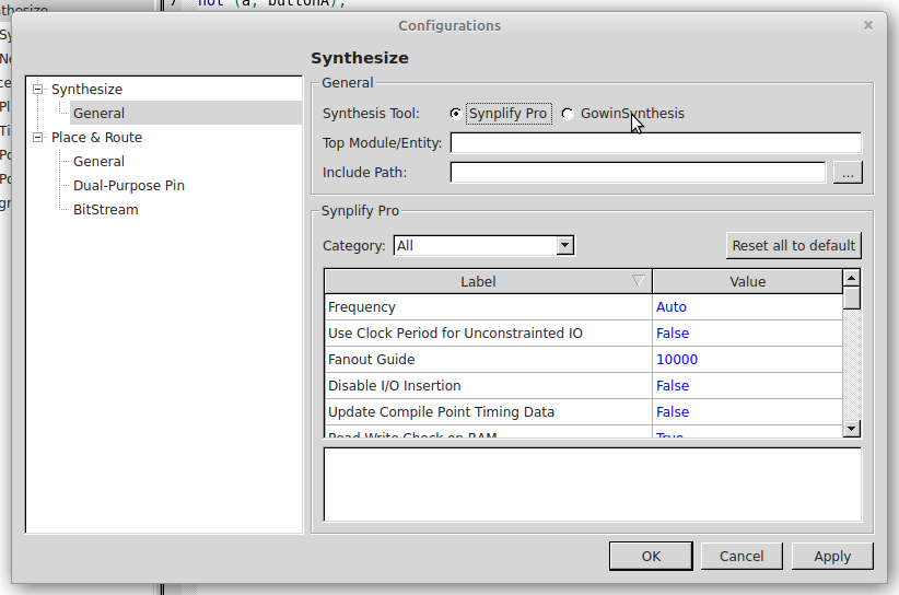
Double click on Synthesize or right click and select Run or Rerun to run the synthesizer. After a few seconds, the icon next to Synthesize should become a tick, indicating that the process has completed. Note that if you chose Synplify Pro in the last step, it may take longer.
Next, double click on FloorPlanner under User Constraints.

In the popup window, click on OK to create a default CST file.
FloorPlanner is a GUI to create physical constraints or map the physical I/O Pins of the FPGA chip to ports in HDL files.
In the FloorPlanner Window, go to Package View. In NetList Panel, find buttonA, buttonB, led under Ports and drag them to the respective Pins on the right based on the schematic we saw just now. We will be using the Green LED. When it is done, the constraints will be shown at the bottom. (buttonA -> 15, buttonB -> 14, led -> 16)
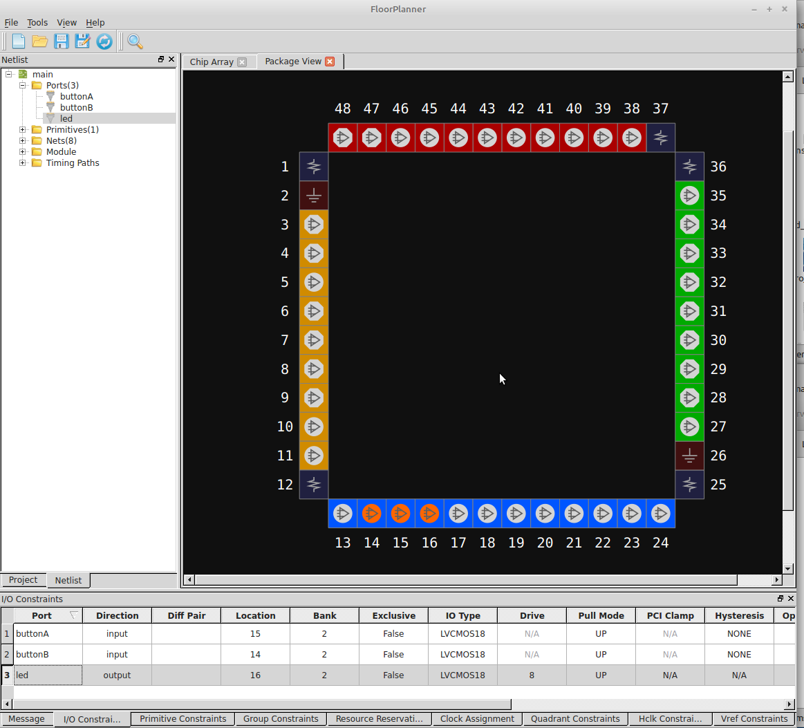
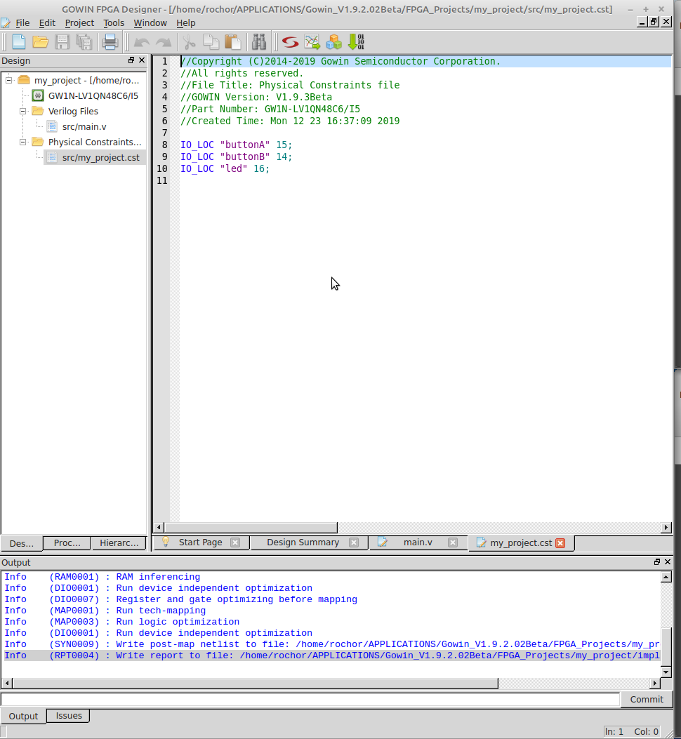
Click on the save button and close FloorPlanner window. You should now see a new .cst file created by FloorPlanner. You can also create the .cst file yourself instead of using FloorPlanner later on.
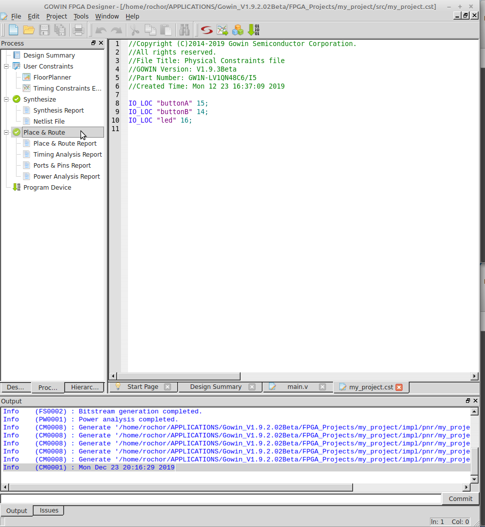
Next, go back to Process panel and double click on Place & Route.
Now it is time to program the chip. We need to use the built-in programmer.
To open the programmer on Windows, either click on Program Device in Process panel or click on the programmer icon in the toolbar at the top.
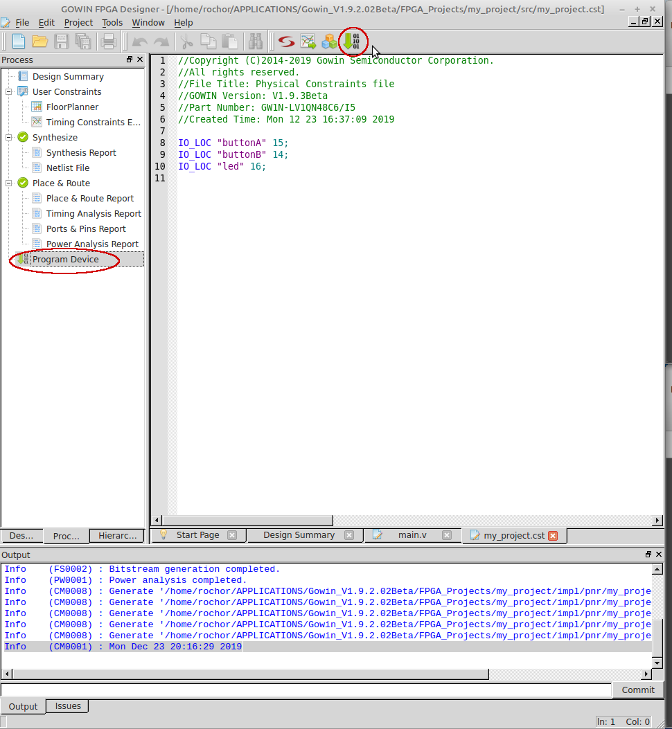
On Linux, you need to run the programmer as root. Thus if you did not start the IDE as root (and you should not do so), you cannot start the programmer from the IDE. Run the following script in your terminal and enter your password.
sudo [Installation-Path]/Programmer/bin/programmer
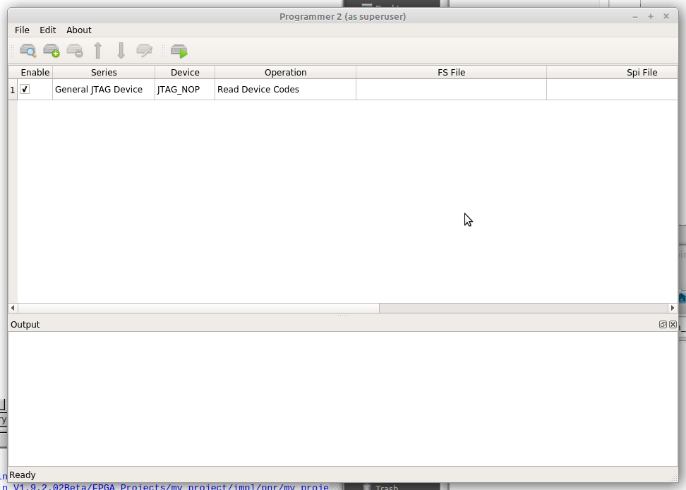
Now, connect the Tang Nano board to your computer through a USB-Type-C cable and click Scan Device in the toolbar. You should then be able to see your board listed below.
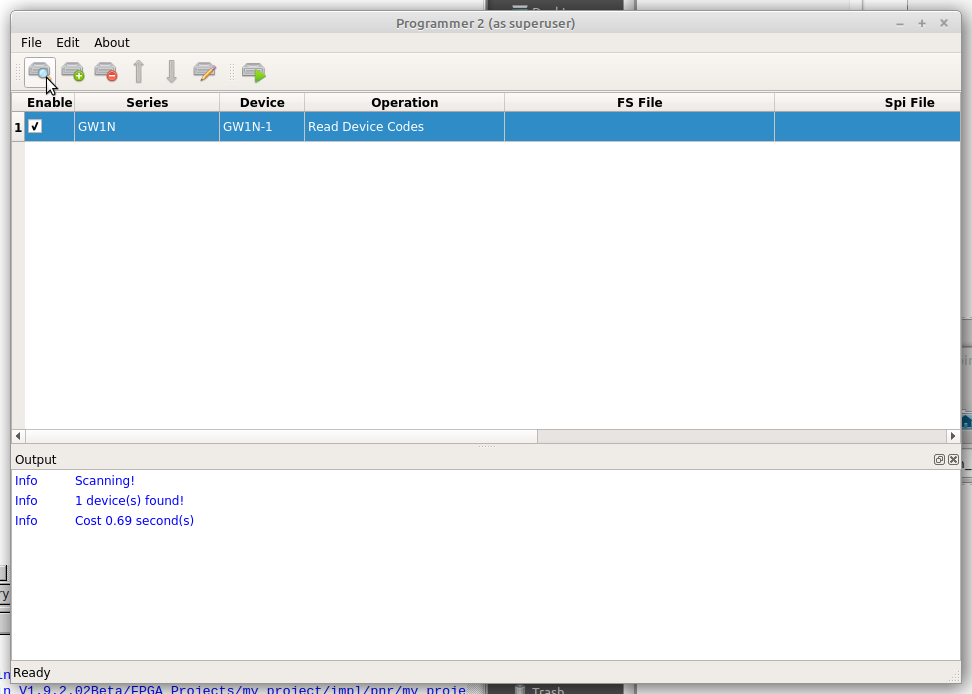
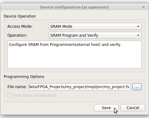
Go to Device Configuration and select SRAM Mode -> SRAM Program and Verify under Device Operation. This will upload the code to the SRAM. It is faster than uploading to flash but the design will not be saved if the board loses power. If you want to save the design, choose embedded flash instead. Under Programming Options, find the .fs file under [project-folder]/impl/pnr. Click on Save to continue.
{% blockquote %}
in cable settings, change frequency to 2.5mhz manually (instead of using the default 2m)!!! Otherwise flashing to embedded flash won't work!
{% endblockquote %}
Click on Program/Configure, wait until the upload and verification process finished.
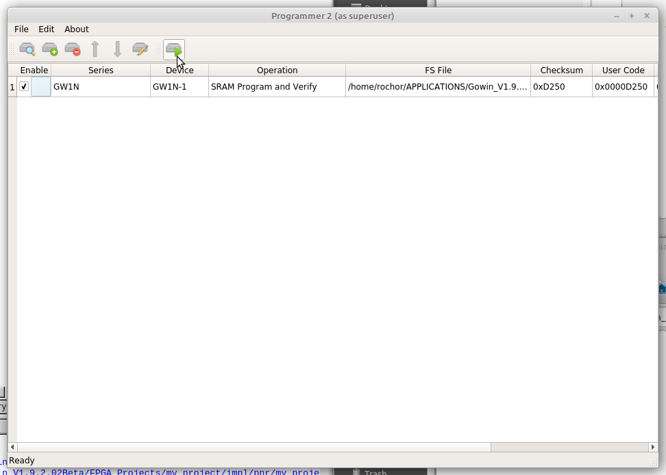
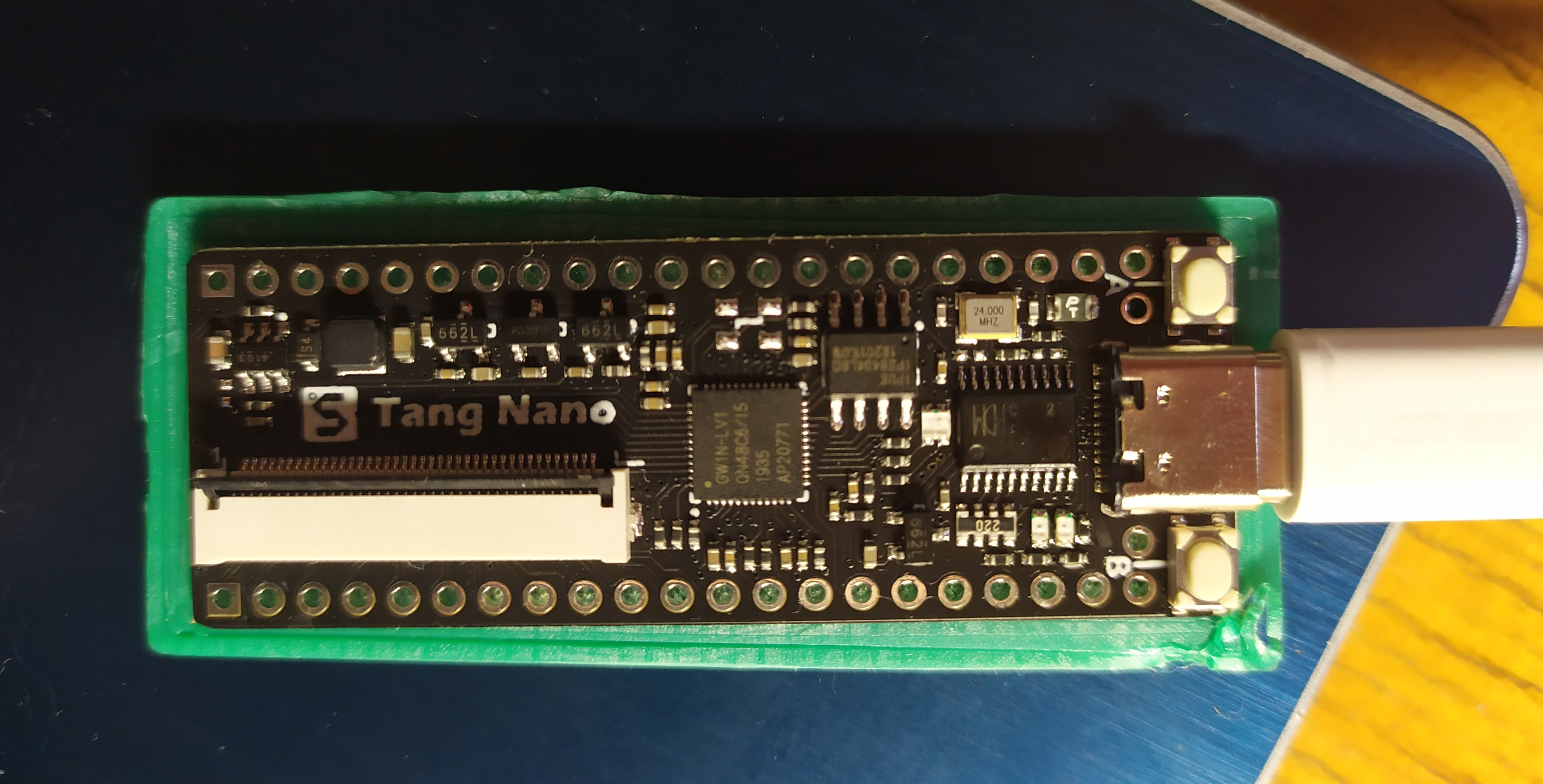
Now the board is loaded with your design. Press the buttons to test it.
 萌ICP备20225200号
Comments